NCP1501
http://onsemi.com
9
APPLICATIONSINFORMATION
NCP1501 is a dual mode PWM or LDO step down
converter.Thisdualmodetakesadvantageofthebestof
eachmode.Therearethreerequiredexternalcomponents:
aninputandoutputcapacitorandaninductor.
ThePWMmodeallowshighefficiencyforlargerloads.
Atypicalefficiencyforaninputof3.6Vandanoutputof
1.8V and 100mA is over 90%. Low R
DSon
and
synchronous rectification contained within the device
contributes to the very high efficiency. As with other
synchronousrectificationdevices,theNCP1501doesnot
requireanexternaldiodetosupplementtheNFETduring
switchingonoroff.Asynchronizationpinallowstheuser
todefinethefrequencynoisespikesofthePWM.Theduty
cycleofthesynchronizationsignalmustbewithintherange
of 30% to 70%. The rising edge of the signal from the
synchronizationpinactsastheoscillatorsignaltosetthe
latch and reset the ramp compensation signal. An Over
VoltageProtectioncircuitensurestheoutputwillrespond
properlytofasttransientsfromlargetosmallloads.The
NCP1501allowsthePWMmodetoentera100%dutycycle
forfastloadtransientconditionsandlowinputtooutput
voltagedifferentials.
TheLDOmodeiseffectiveduringlowloadconditionsby
lowering the quiescent current and reducing the output
ripplevoltageassociatedwithPWMconvertersentering
PFM mode. NCP1501 enters the LDO mode when a
synchronizationsignalisnotpresent.Itisrecommendedto
pullthesynchronizationsignallowforLDOmode.
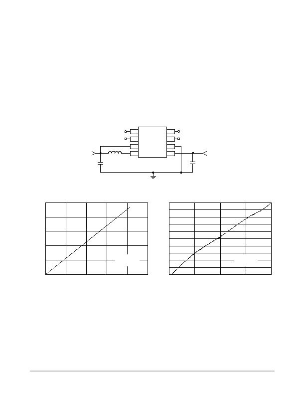
Figure9.TypicalOperatingSchematic
C
out
NCP1501
8
7
6
5
1
2
3
4
SHD
SYN
V
O
LX
CB0
CB1
GND
V
in
C
in
10mH
L
10m
10m
V
bat
V
out
C
in
,C
out
:10mFCeramic,
C2012X5R0J106M(TDK)
L:10mH,LLF4017--100(TDK)
Figure10.InputCurrentversusVoltageforthe
ShutdownPin
5
4
3
2
1
0
V
SHD
(V)
2.5
2
1.5
1
0.5
0
V
CC
=3.6V
T
A
=25癈
Figure11.InputCurrentversusVoltageforthe
SynchronizationPin
4
3
2
1
0
V
SYN
(V)
2
1.8
1.2
1
0.2
0
V
CC
=3.6V
T
A
=25癈
0.4
0.6
0.8
1.4
1.6
发布紧急采购,3分钟左右您将得到回复。
相关PDF资料
NCP1578MNR2G
IC REG DL BCK/LINEAR SYNC 20-QFN
NCP1601BDR2G
IC PFC CTRL CRM/TRANSITION 8SOIC
NCP1603D100R2G
IC CTLR PFC/PWM COMBO 16-SOIC
NCP1605DR2G
IC PFC CONTROLLER CCM/DCM 16SOIC
NCP1606BDR2G
IC POWER FACTOR CONTROLLER 8SOIC
NCP1607BDR2G
IC PFC CONTROLLER CRM 8SOIC
NCP1611BDR2G
IC PFC CTLR HE ENHANCED 8-SOIC
NCP1651DR2G
IC PFC CONTROLLER CCM/DCM 16SOIC
相关代理商/技术参数
NCP1508MNR2
功能描述:直流/直流开关转换器 High Efficiency Buck RoHS:否 制造商:STMicroelectronics 最大输入电压:4.5 V 开关频率:1.5 MHz 输出电压:4.6 V 输出电流:250 mA 输出端数量:2 最大工作温度:+ 85 C 安装风格:SMD/SMT
NCP1508MNR2G
功能描述:直流/直流开关转换器 High Efficiency Buck Synchronous DC/DC RoHS:否 制造商:STMicroelectronics 最大输入电压:4.5 V 开关频率:1.5 MHz 输出电压:4.6 V 输出电流:250 mA 输出端数量:2 最大工作温度:+ 85 C 安装风格:SMD/SMT
NCP1509MNR2
功能描述:直流/直流开关转换器 High Efficiency Buck RoHS:否 制造商:STMicroelectronics 最大输入电压:4.5 V 开关频率:1.5 MHz 输出电压:4.6 V 输出电流:250 mA 输出端数量:2 最大工作温度:+ 85 C 安装风格:SMD/SMT
NCP1509MNR2G
功能描述:直流/直流开关转换器 High Efficiency Buck Synchronous DC/DC RoHS:否 制造商:STMicroelectronics 最大输入电压:4.5 V 开关频率:1.5 MHz 输出电压:4.6 V 输出电流:250 mA 输出端数量:2 最大工作温度:+ 85 C 安装风格:SMD/SMT
NCP1510AFCT1
功能描述:直流/直流开关转换器 High Efficiency Buck RoHS:否 制造商:STMicroelectronics 最大输入电压:4.5 V 开关频率:1.5 MHz 输出电压:4.6 V 输出电流:250 mA 输出端数量:2 最大工作温度:+ 85 C 安装风格:SMD/SMT
NCP1510AFCT1G
功能描述:直流/直流开关转换器 High Efficiency Buck Synchronous DC/DC RoHS:否 制造商:STMicroelectronics 最大输入电压:4.5 V 开关频率:1.5 MHz 输出电压:4.6 V 输出电流:250 mA 输出端数量:2 最大工作温度:+ 85 C 安装风格:SMD/SMT
NCP1510FCT1G
功能描述:直流/直流开关转换器 ANA BUCK REG RoHS:否 制造商:STMicroelectronics 最大输入电压:4.5 V 开关频率:1.5 MHz 输出电压:4.6 V 输出电流:250 mA 输出端数量:2 最大工作温度:+ 85 C 安装风格:SMD/SMT
NCP1511FCT1
功能描述:直流/直流开关转换器 500mA High Frequency RoHS:否 制造商:STMicroelectronics 最大输入电压:4.5 V 开关频率:1.5 MHz 输出电压:4.6 V 输出电流:250 mA 输出端数量:2 最大工作温度:+ 85 C 安装风格:SMD/SMT